- 您现在的位置:买卖IC网 > Sheet目录338 > LT3746IUHH#TRPBF (Linear Technology)IC LED DRIVER 32CHANNEL 56-QFN
�� �
�
�LT3746�
�OPERATION�
�Figure� 2� shows� two� serial� data� input� SDI� frames� (GS� frame�
�and� DC� frame)� and� one� serial� data� output� SDO� frame� (status�
�frame).� All� the� frames� have� the� same� 386-bit� in� length� and�
�are� transmitted� with� the� MSB� first� and� the� LSB� last.� The� SDI�
�frames� are� sent� with� the� SCKI� signal� and� the� SDO� frame� is�
�received� with� the� SCKO� signal.� The� C0� bit� (frame� select)�
�determines� any� SDI� frame� to� be� either� a� GS� frame� (C0� =� 0)�
�or� a� DC� frame� (C0� =� 1),� and� the� C1� bit� (EN)� enables� (C1� =� 1)�
�or� disables� (C1� =� 0)� all� the� LED� channels.� The� status� frame�
�reads� back� the� T� SET� pin� resistor-programmable� over-�
�temperature� flag� and� individual� open/short� LED� fault� flags,�
�as� well� as� the� individual� 6-bit� DC� setting.�
�Inside� the� part,� there� are� one� 386-bit� shift� register�
�SR[0:385],� one� 1-bit� frame� select� (FS)� register,� one� 1-bit�
�enable� LED� channel� (EN)� register,� thirty-two� 12-bit� gray-�
�scale� (GS)� registers,� thirty-two� 6-bit� dot� correction� (DC)�
�registers,� one� 1-bit� over� temperature� (OT)� flag� register,� and�
�thirty-two� 1-bit� LED� fault� flag� registers.� The� input� of� the�
�386-bit� shift� register,� i.e.,� the� input� of� the� first� bit� SR[0],�
�is� connected� to� the� SDI� signal.� The� output� of� the� 386-bit�
�shift� register,� i.e.,� the� output� of� the� last� bit� SR[385]� is� con-�
�nected� to� the� SDO� signal.� The� SCKI� signal� shifts� the� SDI�
�frame� (GS� or� DC� frame)� in� and� the� SCKO� signal� shift� the�
�SDO� frame� (status� frame)� out� of� the� 386-bit� shift� register�
�with� their� rising� edges.� The� LDI� high� signal� latches� the� SDI�
�frame� (GS� or� DC� frame)� from� the� 386-bit� shift� register� into�
�corresponding� FS,� EN,� GS� or� DC� registers,� and� loads� the�
�SDO� frame� (status� frame)� from� the� OT� and� LED� fault� flag�
�registers� to� the� 386-bit� shift� register� at� the� same� time.�
�The� LDO� signal� is� a� buffered� version� of� the� LDI� signal�
�with� certain� delay� added� to� match� the� delay� between� the�
�4096*T� PWMCK�
�SCKI� and� SCKO� signals.� Therefore,� a� daisy-chain� type� loop�
�communication� with� simultaneous� writing� and� reading�
�capability� is� implemented.�
�Figure� 3� illustrates� the� timing� relation� among� serial� input�
�and� serial� output� signals� in� more� detail.� One� DC� frame� fol-�
�lowed� by� another� GS� frame� is� sent� through� the� LDI,� SCKI,�
�and� SDI� signals.� At� the� same� time,� two� status� frames� are�
�received� through� the� LDO,� SCKO,� and� SDO� signals.� The�
�rising� edges� of� the� SCKI� signal� shift� a� frame� of� 386-bit�
�data� at� the� SDI� pin� into� the� 386-bit� shift� register� SR[0:385].�
�After� 386� clock� cycles,� all� the� 386-bit� data� sit� in� the� right�
�place� waiting� for� the� LDI� signal.� An� asynchronous� LDI� high�
�signal� latches� the� 1-bit� FS� register,� 1-bit� EN� register,� and�
�individual� 12-bit� GS� registers� (when� FS� =� 0)� or� 6-bit� DC�
�registers� (when� FS� =� 1)� for� each� channel.� At� the� same� time,�
�a� frame� of� status� information,� including� over� temperature�
�flag� and� individual� open/short� LED� fault� flags,� is� parallel�
�loaded� into� the� 386-bit� shift� register� and� will� be� shifted�
�out� with� the� coming� clock� cycles.�
�Constant� Current� Sink�
�Each� LED� channel� has� a� local� constant� current� sink� regu-�
�lating� its� own� LED� current� independent� of� the� LED� bus�
�voltage� V� OUT� .� The� recommended� LED� pin� voltage� ranges�
�from� 0.5V� to� 2.5V.� As� shown� in� the� Typical� Performance�
�Characteristics� I� LED� vs� V� LED� curves,� the� LED� current� I� LED�
�has� the� best� load� regulation� when� the� LED� pin� voltage� V� LED�
�sits� between� 0.5V� to� 2.5V.� A� lower� LED� bus� voltage� V� OUT�
�may� not� regulate� all� the� LED� channels� across� tempera-�
�ture,� current,� and� manufacturing� variation,� while� a� higher�
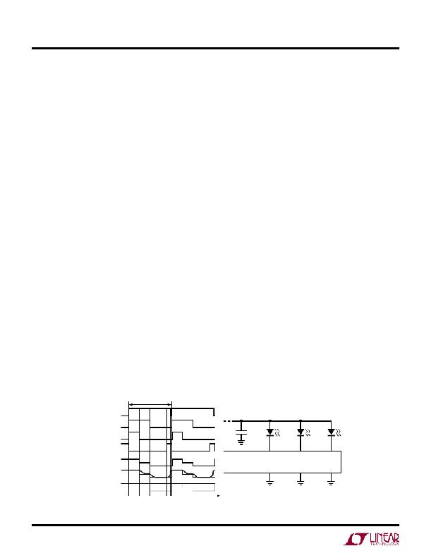
�PWM� 1�
�PWM� 2�
�PWM� 3�
�V� OUT� =� 4.4V�
�3.1V�
�(1)�
�+�
�3.5V�
�(2)�
�+�
�3.9V�
�(3)�
�+�
�PRECHG�
�IDEAL� V� OUT�
�4.4V�
�4.0V�
�3.6V�
�4.4V�
�4.0V�
�3.6V�
�–�
�+�
�1.3V�
�–�
�+�
�0.9V�
�–�
�+�
�0.5V�
�LT3746� V� OUT�
�4.4V�
�–�
�–�
�–�
�CONSTANT� V� OUT�
�3746� F05�
�t� 1�
�t� 2�
�t� 3� t� 4�
�Figure� 5.� Adaptive-Tracking-plus-Precharging� LED� Bus� Voltage� Technique�
�16�
�For� more� information� www.linear.com/3746�
�3746fa�
�发布紧急采购,3分钟左右您将得到回复。
相关PDF资料
LT3754IUH#TRPBF
IC LED DVR 16CH 50MA 32QFN
LT3755EMSE#PBF
IC LED DRVR HP CONS CURR 16-MSOP
LT3760EFE#PBF
IC LED DVR WHT/CLR BCKLT 28TSSOP
LT3799IMSE#PBF
IC LED DRIVER TRIAC DIM 16-MSOP
LT3956EUHE#PBF
IC LED DVR BUCK BOOST 36-VQFN
LTC3201EMS#TRPBF
IC LED DRVR WHITE BCKLGT 10-MSOP
LTC3202EDD#PBF
IC LED DRIVR WHITE BCKLGT 10-DFN
LTC3205EUF#TRPBF
IC LED DRVR WT/RGB BCKLGT 24-QFN
相关代理商/技术参数
LT3748
制造商:LINER 制造商全称:Linear Technology 功能描述:Monolithic High Voltage Isolated Flyback Converter No External Start-Up Resistor
LT3748_1
制造商:LINER 制造商全称:Linear Technology 功能描述:100V Isolated Flyback Controller
LT3748EMS#PBF
功能描述:IC REG CTRLR FLYBK ISO CM 16MSOP RoHS:是 类别:集成电路 (IC) >> PMIC - 稳压器 - DC DC 切换控制器 系列:- 标准包装:4,500 系列:PowerWise® PWM 型:控制器 输出数:1 频率 - 最大:1MHz 占空比:95% 电源电压:2.8 V ~ 5.5 V 降压:是 升压:无 回扫:无 反相:无 倍增器:无 除法器:无 Cuk:无 隔离:无 工作温度:-40°C ~ 125°C 封装/外壳:6-WDFN 裸露焊盘 包装:带卷 (TR) 配用:LM1771EVAL-ND - BOARD EVALUATION LM1771 其它名称:LM1771SSDX
LT3748EMS#TRPBF
功能描述:IC REG CTRLR FLYBK ISO CM 16MSOP RoHS:是 类别:集成电路 (IC) >> PMIC - 稳压器 - DC DC 切换控制器 系列:- 标准包装:2,500 系列:- PWM 型:电流模式 输出数:1 频率 - 最大:500kHz 占空比:96% 电源电压:4 V ~ 36 V 降压:无 升压:是 回扫:无 反相:无 倍增器:无 除法器:无 Cuk:无 隔离:无 工作温度:-40°C ~ 125°C 封装/外壳:24-WQFN 裸露焊盘 包装:带卷 (TR)
LT3748EMSPBF
制造商:Linear Technology 功能描述:100V Isolated Flyback Controller MSOP16
LT3748EMSTRPBF
制造商:LINER 制造商全称:Linear Technology 功能描述:100V Isolated Flyback Controller
LT3748HMS#PBF
功能描述:IC REG CTRLR FLYBK ISO CM 16MSOP RoHS:是 类别:集成电路 (IC) >> PMIC - 稳压器 - DC DC 切换控制器 系列:- 特色产品:LM3753/54 Scalable 2-Phase Synchronous Buck Controllers 标准包装:1 系列:PowerWise® PWM 型:电压模式 输出数:1 频率 - 最大:1MHz 占空比:81% 电源电压:4.5 V ~ 18 V 降压:是 升压:无 回扫:无 反相:无 倍增器:无 除法器:无 Cuk:无 隔离:无 工作温度:-5°C ~ 125°C 封装/外壳:32-WFQFN 裸露焊盘 包装:Digi-Reel® 产品目录页面:1303 (CN2011-ZH PDF) 其它名称:LM3754SQDKR
LT3748HMS#TRPBF
功能描述:IC REG CTRLR FLYBK ISO CM 16MSOP RoHS:是 类别:集成电路 (IC) >> PMIC - 稳压器 - DC DC 切换控制器 系列:- 标准包装:4,500 系列:PowerWise® PWM 型:控制器 输出数:1 频率 - 最大:1MHz 占空比:95% 电源电压:2.8 V ~ 5.5 V 降压:是 升压:无 回扫:无 反相:无 倍增器:无 除法器:无 Cuk:无 隔离:无 工作温度:-40°C ~ 125°C 封装/外壳:6-WDFN 裸露焊盘 包装:带卷 (TR) 配用:LM1771EVAL-ND - BOARD EVALUATION LM1771 其它名称:LM1771SSDX